In some communication circuits, a phase Compensation FIFO is used to transfer data between two clock domains, which are totally frequency equal but different phase drifts. For example, clock a(WCLK) and clock b(RCLK), have the same frequency but their phases are drafted. The shifted amount and direction are unknown. The data are sent and latch at every rising edge of clocks from WCLK to RCLK. To safely transfer data from WCLK side to RCLK side, some of technical tips shall consider.
Since data send at every clock cycle to cross clock domains, a synchronous FIFO shall use.
The FIFO depth is at least 2. This is to avoid reading data that just writing in, which can cause metastability issue if two clock phases are closed. Also, the FIFO operation shall make sure to read one entry of data that has been write into FIFO one cycle ago. If read the data just written in, metastability issue can happen. For example, when write data into FIFO entry 0, it shall read from FIFO entry 1. And vice versa, when write into FIFO entry 1, it shall read from FIFO entry 0. How to make sure such operation is tricky since there is not time to exchange full and empty flags between two clock domains (it supposed the exchange the full and empty flags go through synchronizers).
The diagram shows here a conventional asynchronous FIFO architecture. The write side uses a write point to count which FIFO entry the data written into while the read side use a read point to count which FIFO entry the data read from.
Supposed the data keep streaming, the lost data at the beginning and the end of transaction is acceptable. So to align the FIFO operation is dependent on the when to release the reset signals for both write and read logic.
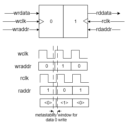
As above diagram, it reviews three cases. One is the rising edge of WCLK is ahead of the rising edge of RCLK, one is WCLK is ahead of RCLK about half cycle, the last one is WCLK is after of RCLK. Three cases prove that reading at the alternative address from writing can avoid the metastability issue. To make sure the write point and read point running on alternative address, the problem becomes when to start counting the both address points.
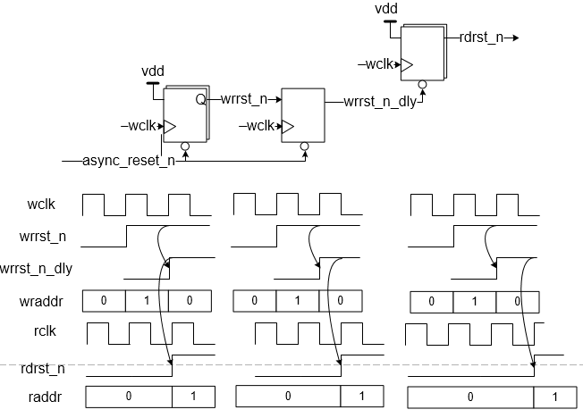
As in above diagram, by delay, wrrst_n, the reset signal of write side one WCLK cycle, the reset logic in above diagram makes sure the read point at the read side is one cycle after write side, so the read point is one cycle later than the write point, which eventually makes the read and write running at alternative address. Also, the three cases are checked with waveform.
